

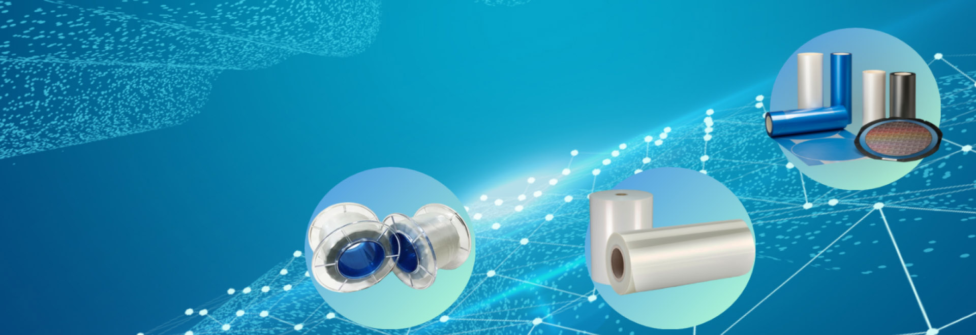
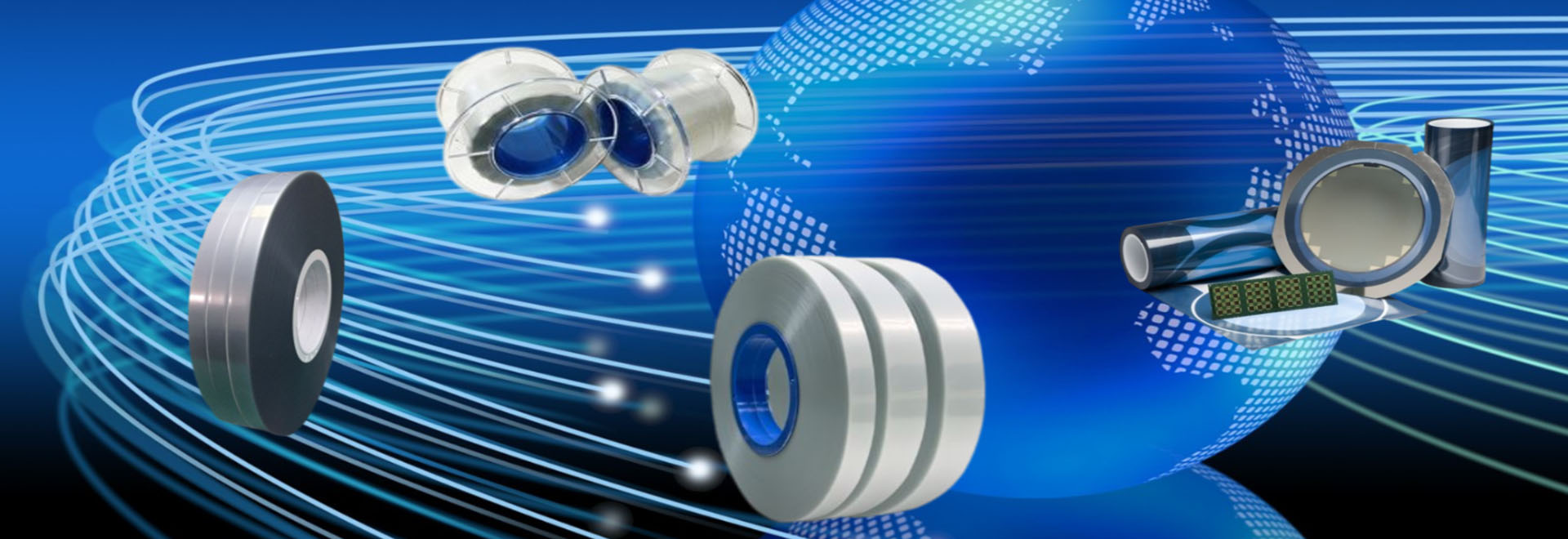
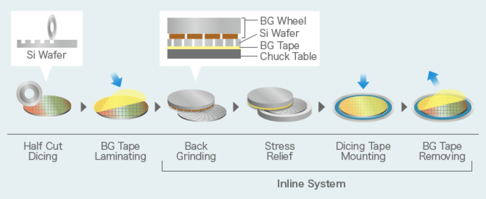
Wafer dicing is a crucial process in the semiconductor packaging industry, used to separate silicon wafers into individual chips. This step is an essential part of the multi-stage manufacturing process that transforms raw materials into packaged devices configured for electronic circuits.
Process Overview
1. Preparation:
Wafers are mounted on PVC or Mylar tape with adhesive backing
The tape is secured to a metal frame for stability
The entire process occurs in a clean room to prevent contamination by minute particles
2. Dicing Methods:
Blade dicing: Uses a diamond-coated blade
Laser dicing: Employs a high-powered laser
Stealth dicing: Utilizes laser-induced internal stress for cleaner separation
3. Tape Selection:
UV-curable tapes for smaller die sizes
Non-UV dicing tapes for larger die sizes
4. Die Shapes:
Typically rectangular or square
Can vary based on the dicing method used
Market Drivers
1. Increasing integration of microelectronics in consumer electronics
2. Growing demand for thin wafers in MEMS devices and power devices
3. Need for improved manufacturing processes for ultra-thin wafers
Key Application Areas
Radio Frequency Identification (RFID) technology
Micro-Electro-Mechanical Systems (MEMS) devices
Power devices
Industry Trends
As wafers become thinner and chip sizes continue to shrink, the dicing process faces new challenges. This drives continuous innovation in dicing technologies and equipment to achieve more precise and efficient chip separation while ensuring the integrity of delicate circuits.
The optimization of the wafer dicing process directly impacts the yield and quality of the final product, making it an indispensable step in semiconductor manufacturing. At Nexteck, we understand the importance of this critical process and strive to provide reliable solutions that meet the evolving needs of the semiconductor industry.
Our team at Nexteck is committed to staying at the forefront of wafer dicing technology, continuously refining our processes and equipment to help our clients achieve optimal results in their semiconductor manufacturing endeavors.


