Wafer (Silicon Wafer)
We are proud of offering silicon wafer with high quality and attractive price under quality control in depth so that you are assured high value added products from us. Our main product series include: IC level and solar grade silicon ingot and wafers.
IC level ingots and wafers:
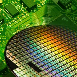
![]() can provide you semiconductor wafer measured from four to six inches. The specifications are as follows:
can provide you semiconductor wafer measured from four to six inches. The specifications are as follows:
| Category | General Specification of Semiconductor Wafer | ||||||||
| 4 inch | 5 inch | 6 inch | |||||||
| Resistivity(Ω/cm) | P-Type doped: Boron, 0.001-0.01, 0.01-0.5, >0.5 P++, P+, P- | ||||||||
| N-Type doped: As, Phos, Sb, 0.001-1, 1-150 | |||||||||
| Diameter tolerance(mm) | ±0.2 | ±0.2 | ±0.2 | ||||||
| Orientation | (100), (111) | (100), (110), (111) | (100), (110), (111) | ||||||
| Orientation tolerance | ±0.15° | ±0.15° | ±0.15° | ||||||
| Edge Profile | T/R | T/R | T/R | ||||||
| Edge Condition | 11/22 Ground | 11/22 Ground | 11/22 Ground/Polished | ||||||
| Thickness(μm) | 300-650 | 400-650 | 550-750 | ||||||
| Thickness tolerance(μm) | ±15 | ±15 | ±15 | ||||||
| Backside Treatment | Etch | Poly | SiO2 | Etch | Poly | SiO2 | Etch | Poly | SiO2 |
| Bow(μm) | ±25 | ±25(Before CVD) | ±25 | ±25(Before CVD) | ±25 | ±25(Before CVD) | |||
| Warp(μm) | ≦25 | ≦25(Before CVD) | ≦25 | ≦25(Before CVD) | ≦25 | ≦25(Before CVD) | |||
| Options | Laser marking, Poly-back, SiO2 seal, Back side damage | ||||||||
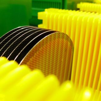
can offer many different kind of ingots and wafers as customer’s requirements. MONO and MULTI ingots or 125mm and 156mm wafers are available to supply.
Below is some specifications of our 156mm Mono and Multi silicon wafers for your reference.
| Specification of 156 mm Mono silicon wafer | Specifications of 156 mm Multi wafer | |
| Category | 156*156mm(Mono wafer) | 156*156mm (multi wafer) |
| Growing method | CZ | CZ |
| Type | P | P |
| Dopant | Boron | Boron |
| Crystal Orientation | <100>+/-3 deg | |
| Carbon content (atom/cm3) | < 5*1016 | < 5*1017 |
| Oxygen content (atom/cm3) | < 1.1*1018 | < 1*1018 |
| Etch Pit Defects ( /cm3) | <= 3000 | |
| Resistivity (ohm-cm) | 0.5~3/3~6 | 0.5~3 |
| Minorirty Carrier Lifetime (μs) | >10 | >=2 |
| Dimension (mm) | 156+/-0.5 | 156+/-0.5 |
| Thickness (μm) | 200+/-20 | 200+/-20 |
| TTV (μm) | <=30 | <=30 |
| Bow/Warp (μm) | <100 | <50 / <100 |
| Surface Saw Damage Depth (um) | <=15 | <=20 |
| Edge (Chip) |
Depth≦0.5mm, Vertical≦1.0mm, Defect≦2 |
Depth≦0.5mm, Length≦3.0mm, Defect≦2 |
| Appearance | As cut, as clean, no cracks | As cut, as clean, no cracks |