Welcome To NEXTECK
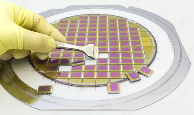
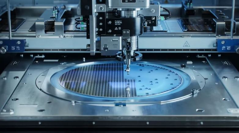
The Dicing process is mostly used in the semiconductor packaging industry to separate Silicon wafers into individual chips. The Integrated Circuits are manufactured in a multistep process that converts raw materials into packaged devices that may be configured into electronic circuits. In other words, it is a process by which the separation of the die from the silicon wafer is referred to as the Dicing process. During the Dicing process, Wafers are mounted using PVC or Mylar tape, which has a sticky backing and holds the wafer on a metal frame. Because even the smallest dust particles might damage the complicated circuits imprinted on a wafer, the process is done in a clean area with air constantly circulating. This tape has different properties depending on its application. For smaller die sizes, UV curable tapes are used, while non-UV dicing tape is used for bigger die sizes. When a wafer is diced, the die remains on the Mylar tape until it is retrieved by the equipment, such as a die bonder. The dies are most commonly rectangular or square. Depending on the Dicing method used, they can also be other shapes.

The dicing equipment market is getting pace due to the integration of microelectronics in consumer electronics. The demand for thin wafers is being driven by the necessity for technologies such as MEMS devices and power devices. Furthermore, this need supports the desire for improved manufacturing methods, which is a critical stage in the ultra-thin wafer manufacturing process. Radio Frequency Identification, MEMS devices, and power devices are considered to be the primary sources of demand for very thin wafers. This scenario is increasing demand for a better manufacturing process, specifically for processing and dicing, which are crucial stages in the creation of ultra-thin wafers.
